Equipment-OLD
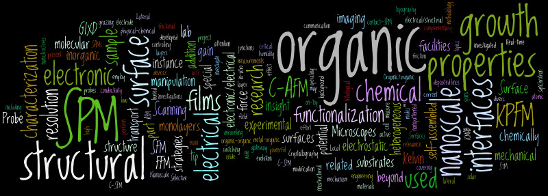
Our lab counts with two scanning force microscopes (SFMs) operating in ambient and nitrogen atmosphere which are dedicated to the investigation of the electronic/electrical properties (C-SFM, KPFM) and mechanical properties (friction, adhesion, elasticity) with nanoscale resolution. SFM measurements can be performed for “in-operando” devices, in particular OFETs, having access to the correlation between nanoscale properties and device performances.
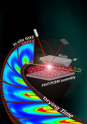
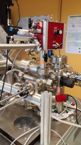
We have two portable UHV chambers for organic film growth from the vapour phase, equiped with different evaporators and electrical in-situ transport measurements. These chambers are furnished with beryllium windows to allow real-time growth studies by X-ray diffraction at synchrotron light facilities.
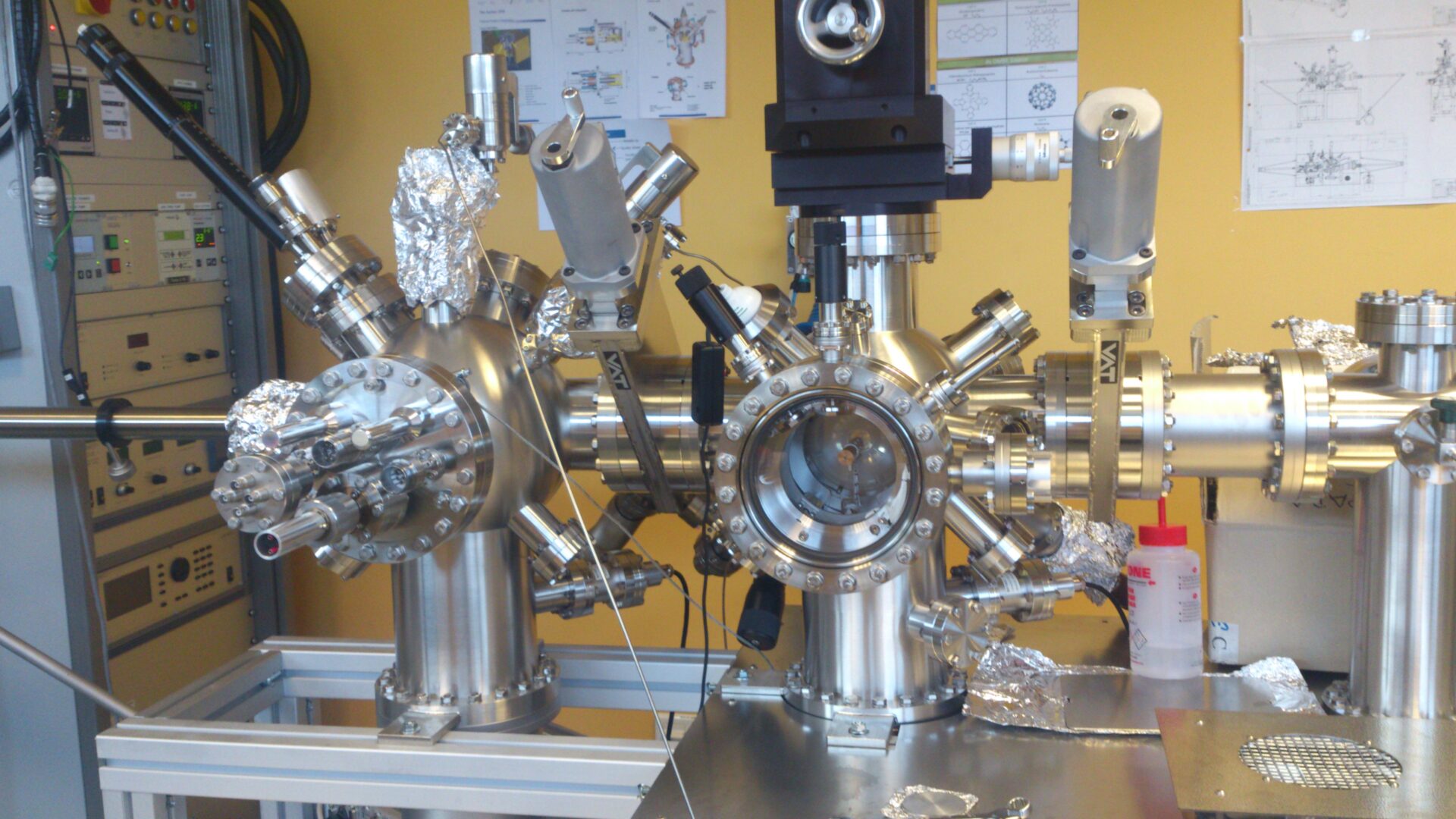
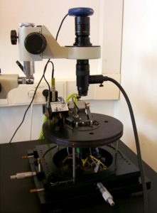
We also have a SPM Aarhus 150 with KolibriSensor that enables simultaneous non-contact atomic force microscopy (NC-AFM) and scanning tunneling microscopy (STM) operation in UHV environment (base pressure 5×10⁻¹⁰ mbar) and variable temperature. This equipment allows exploring electronic properties of organic heterojunctions and interfaces at molecular level. The whole instrument consists of preparation and characterization chambers plus a lock-load chamber for fast sample introduction. This lab is settled at the Synchrotron Light Facility ALBA.
A pulse-injection system (ALI, BihurCrystal) is mounted in connection to the NC-AFM/STM UHV chamber for deposition of molecules from solutions. The solution is introduced in a pre-injection system and, using an inert carrier gas, is injected through a pulsed valve into the UHV chamber hosting the sample. The solute travels within the microdrops being deposited on the sample surface. Full control over the spray process allows easily recovering working pressures (~10-8 mbar), leading to a thin, pollutant-free layer of the solute on the sample, ready for characterization in UHV environment.
In addition, the equipment counts with a suitcase (or portable chamber) that allows sample transfer under the UHV conditions for further characterization in other external equipments or at different beamlines of ALBA.