People
————
————
————
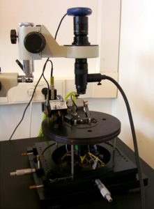
Our lab counts with two scanning force microscopes (SFMs) operating in ambient and nitrogen atmosphere which are dedicated to the investigation of the electronic/electrical properties (C-SFM, KPFM) and mechanical properties (friction, adhesion, elasticity) with nanoscale resolution. SFM measurements can be performed for “in-operando” devices, in particular OFETs, having access to the correlation between nanoscale properties and device performances.
We have two portable UHV chambers for organic film growth from the vapour phase, equiped with different evaporators and electrical in-situ transport measurements. These chambers are furnished with beryllium windows to allow real-time growth studies by X-ray diffraction at synchrotron light facilities.
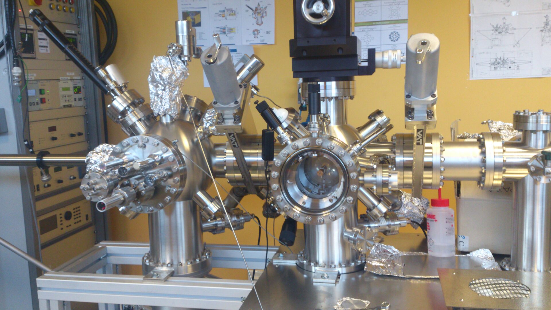
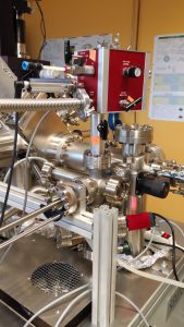
We also have a SPM Aarhus 150 with KolibriSensor that enables simultaneous non-contact atomic force microscopy (NC-AFM) and scanning tunneling microscopy (STM) operation in UHV environment (base pressure 5×10⁻¹⁰ mbar) and variable temperature. This equipment allows exploring electronic properties of organic heterojunctions and interfaces at molecular level. The whole instrument consists of preparation and characterization chambers plus a lock-load chamber for fast sample introduction. This lab is settled at the Synchrotron Light Facility ALBA.
A pulse-injection system (ALI, BihurCrystal) is mounted in connection to the NC-AFM/STM UHV chamber for deposition of molecules from solutions. The solution is introduced in a pre-injection system and, using an inert carrier gas, is injected through a pulsed valve into the UHV chamber hosting the sample. The solute travels within the microdrops being deposited on the sample surface. Full control over the spray process allows easily recovering working pressures (~10-8 mbar), leading to a thin, pollutant-free layer of the solute on the sample, ready for characterization in UHV environment.
In addition, the equipment counts with a suitcase (or portable chamber) that allows sample transfer under the UHV conditions for further characterization in other external equipments or at different beamlines of ALBA.
Two-dimensional organic hybrid structures for artificial photosynthesis
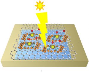
The conversion of solar energy to chemical energy represents one of the most attractive prospects to solve the global energy and environmental challenges exisiting nowadays. Artificial photosynthesis aims to mimic the natural model, which, in essence, uses molecular systems to harvest sunlight, to oxidize water and to drive a cascade of electron and energy transfer reactions. The basic principles involve the capture of solar energy, the transfer of the excitation energy to special locations- the reaction centers- and the charge separation for the subsequent electron-transfer processes. Many challenges persist in achieving the desired goal of cheap and efficient conversion of solar energy into chemical energy and, still very little information is available at atomic-scale about the behaviour of water at interfaces of different nature and about the specific interactions involved.
This project focuses on the exploration of novel two-dimensional heterostructures based on organic assemblies and graphene with potential application in photocatalysis and artificial photosynthesis. The study aims at understanding fundamental interface phenomena related with the structure and the photochemistry of these 2D systems, at atomic-scale level. The experimental methods to use are Scanning Tunneling Microscopy and Frequency Modulation Atomic Force Microscopy (STM/FM-AFM) in Ultra-High Vacuum (UHV) complemented by near-ambient pressure X-ray techniques (XPS/NEXAFS) performed at the ALBA Synchrotron Light Source.
We are searching well-qualified and highly motivated PhD candidates who wishes to work in a stimulating environment as well as to obtain a doctoral degree in physics or materials science. Eligibility requires an internationally-recognized Master-equivalent degree, an excellent academic record and good knowledge of English.
Benefits
DOC-FAM doctoral programme promotes adequate work and employment conditions for the recruited researchers, fulfilling the principles set in the Charter & Code. Selected fellows will receive a generous salary including living and mobility allowances. In addition, DOC-FAM will cover tuition fees for PhD studies during the 3 years of the contract. Fellows will also enjoy research, training & networking costsrelated to their participation in the different activities throughout the programme.
Living allowance: 28,800€/year
Mobility allowance: 4,800€/year
TOTAL gross salary*: 33,600€/year
*Net salary results from deducting all compulsory social security contributions as well as direct taxes from the gross amounts. Social security coverage for the contracted fellows in Spain include benefits for health care, occupational accident, unemployment and disablement benefits, parental and sick leave.
Contact:
This group started up its activity at the ICMAB in 2007. Our research is focused on unraveling and controlling the nanoscale structural and electronic properties of nanostructures and interfaces through surface engineering. Devoting special effort to organic materials, part of our investigation centers on organic semiconductors with relevance as active layers for electronic devices (such as organic solar cells and organic field effect transistors). Surfaces and interfaces (organic-organic and organic-inorganic) are of critical importance because they are the gateway for electrical communication and, in addition, they largely influence the structural properties of on-top deposited semiconductor organic layers. In this regard, another part of our research focuses on the characterization and manipulation of the nanoscale electrical/structural properties of interfaces.

former PhD. Student
ITN SEPOMO